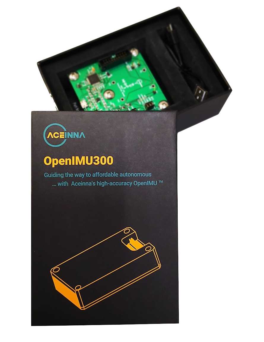
OpenIMU330BI Eval Kit
The OpenIMU330BI evaluation kit consists of a robust and easy-to-use eval board, a test fixture, the OpenIMU330BI IMU module, and an ST-LINK J-TAG pod.
OpenIMU330BI Overview
1. Introduction
The OpenIMU evaluation kit is a hardware platform to evaluate the OpenIMU330BI inertial navigation system and develop various applications based on this platform. Supported by the Aceinna Navigation Studio the kit provides easy access to the features OpenIMU330BI and explains how to integrate the device in a custom design. The OpenIMU evaluation kit include OpenIMU330BI, evaluation board with various interface connectors and test adapter for mounting OpenIMU330BI unit.

2. Components
OpenIMU Evaluation board, which includes:
- Virtual COM-port USB interface, providing connectivity to OpenIMU330BI unit from PC
- Connector for programming and debugging target via Serial Wire Debug (SWD) interface
- Connector for interfacing OpenIMU330BI from custom-designed system.
- Test terminals for connecting oscilloscope or logic analyzers to the dedicated OpenIMU330BI signals.
OpenIMU330BI unit. Please note, that it installed on the bottom side of evaluation board.
Test fixture adapter for convenient aligned mounting of OpenIMU evaluation board and OpenIMU330BI unit
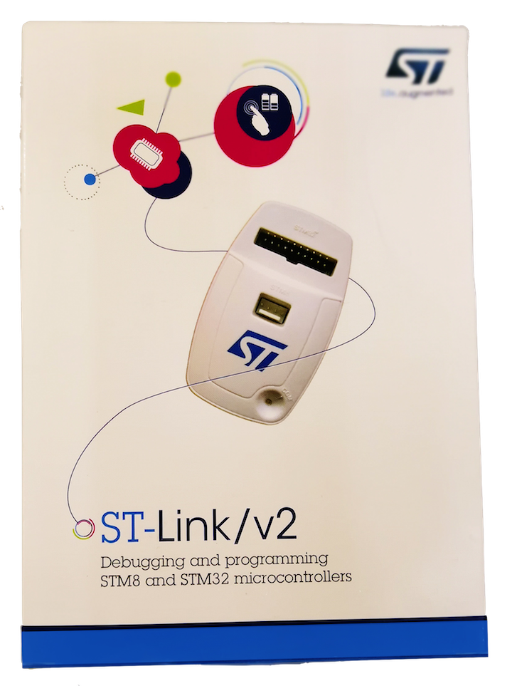
ST-Link debugger for in-system development of application code
2.1 OpenIMU330BI unit
OpenIMU330BI is 9 DOF (degrees of freedom) fully calibrated tripple redundant inertial unit. It is used as the base for development custom inertial navigation applications.
2.2 OpenIMU Evaluation board
OpenIMU Evaluation board designed to provide convenient way for communicating with OpenIMU330BI unit from PC, to expose serial and SPI interfaces to developer and to debug applications using ST-Link debugger vis SWD interface.
2.3 OpenIMU test adapter
OpenIMU test adapter used to firmly secure OpenIMU330BI unit and Open IMU evaluation board in precisely aligned position.
2.4 ST-Link debugger
St-Link debugger is standard debugger provided by STMicroelectronics company. It used for in-system debugging of applications via SWD interface.
3. Open IMU evaluation board Headers and Connectors
3.1 Connector for plugging in OpenIMU330BI unit (J2).
J2 is 20-pin connector and it used for connecting the OpenIMU330BI unit into Open IMU evaluation board. The pin functions are described in the table on the “OpenIMU Modules » OpenIMU330BI - EZ Embed Automotive Module » Connector Pinout - Including GPS Sensor Interface” page accessible from the Contents bar on the left.
3.2 Extension Header (P4)
OpenIMU evaluation board has 12-pin extension header. It designed to expose IMU interface signals to external system. The extension header pin functions described in table below
Pin Main Function Alternative Function 1 Power GND Power GND 2 Power GND Power GND 3 4 5 6 1PPS Input from GPS 7 8 External Reset (NRST)) 9 10 GPIO Output (IO2) GPIO Input 11 Power VIN 5 VDC Power VIN 5 VDC 12 GPIO Output (IO3) GPIO Input 17 19 3.4 IMU interface type selection header (P1).
Pins 1-2 define IMU Interface Mode:
If there is no connection between pins 1 and 2 (jumper is OFF) - SPI mode.if there is connection between pins 1 and 2 (jumper is ON) - UART mode (default).In SPI mode:
Jumpers between pins 3-4 and 5-6 need to be taken OFF to prevent interference between SPI bus signals (SS and MISO) and serial interface signals from FTDI chip.IMU SPI interface signals (MISO, MOSI, SS, SCK, DRDY) routed to header P4.
Note
On SPI interface IMU acts as a SLAVE device.
Note
Not all provided application examples support SPI interface mode. Please refer to specific example for details.
In UART mode:
Jumper between pins 3-4 should be “ON” (default) if IMU Serial Channel 0 ( USER main channel ) needs to be routed to PC via USB connection (on first in the row enumerated USB virtual COM port. See p.6).Jumper between pins 3-4 should be OFF if IMU Serial Channel 0 needs to be accessed from P2 connector.3.5 IMU Serial Debug Channel mode selection header (P2).
Jumpers between pins 1-2 and 3-4 should be ON if IMU Debug Serial needs to be routed to PC via USB connection, for example in case of using IMU Debug Serial Channel for streaming out debug information to PC or as CLI interface (on third in the row enumerated USB virtual COM port. See p.6).Jumpers between pins 1-2 and 3-4 should be OFF if IMU Debug Serial Channel needs to be routed to some external device (for example GPS). In this case pin 2 is RX (to IMU) and pin 4 is TX (from IMU).3.6 SWD (JTAG) connector (P3).
20-pin connector P3 used for connecting ST-Link or J-Link debuggers to the IMU for in-system debugging of applications via SWD interface. It has standard pin-out.
Pin Main Function 1, 2 Vref 4, 6, 8, 10 , 12, 14, 16, 18, 20 GND 7 SWDIO 9 SWCLK 15 nRST 19 3.3V from debugger 3.7 USB connector (J3)
USB connector used for powering up the IMU and evaluation board. Also its used to providing connectivity from PC to IMU via virtual serial ports. Up to 3 exposed IMU serial interfaces can be routed to PC.
4. OpenIMU evaluation board LED indicators
Evaluation board has few LED indicators for visual monitoring of data traffic on serial ports:
LED2 indicator reflects activity on RX line of IMU main (user) serial interface (traffic to IMU)
LED1 indicator reflects activity on TX line of IMU main (user) serial interface (traffic from IMU)
LED3 indicator while lit indicates presence of the power (in case switch SW1 is “ON”)
LED4 indicator reflects activity on GPIO3 (lit if high)
LED5 indicator reflects activity on GPIO2 (lit if high)
5. Open IMU evaluation board power
Power to OpenIMU evaluation board provided by USB. To power system up - connect USB cable to connector J1 and turn “ON” switch SW1.
6. Communication with IMU from PC
The OpenIMU evaluation board has an FTDI chip FT4232 installed. This chip provides 4 virtual serial ports. When evaluation board set up to force IMU interface in UART mode (see p.3.4) up to 3 serial ports on IMU can communicate with PC. When evaluation board connected to PC and power switch turned “ON” in Device Manager board will appear as 4 new consecutive virtual COM ports.First in a row virtual port is routed to IMU’s main UART channel (Serial channel 0) (pins 3 and 4 on J2), and usually dedicated for sending commands to IMU and capturing responses and periodic messages from IMU. It usually used by python driver to establish communication between IMU and Aceinna Navigation Studio.Third in a row virtual port routed to IMU’s Debug Serial Channel (pins 17 and 19 on J2) and usually used as a debug/CLI serial channel .
OpenIMU330BI Evaluation Kit Setup
- Unpack OpenIMU330BI evaluation kit.
- Push power switch to “OFF” position.
- Connect OpenIMU330BI evaluation board to the PC via USB cable. USB connection provides power to the test setup as well as connectivity between PC and IMU serial ports.
- Connect ST-Link debugger to the PC via USB cable.
- Connect OpenIMU330BI evaluation board to ST-Link debugger using provided 20-pin flat cable.
- Push power switch to “ON” position.
Now you are ready to debug and test your application.
- The following activities are addressed in the “Development Tools” section:
- Download App with JTAG
- Debugging with PlatformIO Debugger and JTAG Debug Adapter
- Graphing & Logging IMU Data using the Acienna Navigation Studio
OpenIMU Evaluation Kit Important Notice
This evaluation kit is intended for use for FURTHER ENGINEERING, DEVELOPMENT,
DEMONSTRATION, OR EVALUATION PURPOSES ONLY. It is not a finished product and may not (yet)
comply with some or any technical or legal requirements that are applicable to finished products,
including, without limitation, directives regarding electromagnetic compatibility, recycling (WEEE),
FCC, CE or UL (except as may be otherwise noted on the board/kit). Aceinna supplied this board/kit
"AS IS," without any warranties, with all faults, at the buyer's and further users' sole risk. The
user assumes all responsibility and liability for proper and safe handling of the goods. Further,
the user indemnifies Aceinna from all claims arising from the handling or use of the goods. Due to
the open construction of the product, it is the user's responsibility to take any and all appropriate
precautions with regard to electrostatic discharge and any other technical or legal concerns.
EXCEPT TO THE EXTENT OF THE INDEMNITY SET FORTH ABOVE, NEITHER USER NOR ACEINNA
SHALL BE LIABLE TO EACH OTHER FOR ANY INDIRECT, SPECIAL, INCIDENTAL, OR
CONSEQUENTIAL DAMAGES.
No license is granted under any patent right or other intellectual property right of Aceinna covering
or relating to any machine, process, or combination in which such Aceinna products or services might
be or are used.
Note
In OpenIMU330BI EVK by default signs of readings on X and Z axes are flipped in comparison to the Coordinate Frame drawing on top of the EVK board since OpenIMU330BI unit mounted upside-down in the EVK.