OpenIMU SPI Messaging Framework
1. Introduction
OpenIMU supports a SPI interface for data communications as a one of the choices. To enforce SPI interface mode ‘Data Ready’ signal needs to be forced HIGH of left unconnected on system startup. OpenIMU SPI interface signals described here.
OpenIMU operates as a slave device.
2. OpenIMU SPI communication model
OpenIMU has 128 8-bit registers accessible via SPI interface for reading and writing. The usage of these registers is completely user-defined in time of FW development. Access to the few registers is implemented in the examples as a reference:
Table 1. SPI registers used in the examples
Function Notes 4,5 (0x04, 0x5) r r X-Rate MSB in reg.4 (Note 1) 6,7 (0x06, 0x7) r r Y-Rate MSB in reg.6 (Note 1) 8,9 (0x08, 0x9) r r Z-Rate MSB in reg.8 (Note 1) 10,11 (0x0A, 0xB) r r X-Accel MSB in reg.10 (Note 2) 12,13 (0x0C, 0xD) r r Y-Accel MSB in reg.12 (Note 2) 14,15 (0x0E, 0xF) r r Z-Accel MSB in reg.14 (Note 2) 16,17 (0x10, 0x11) r N/A X-MAG MSB in reg.16 (Note 3) 18,19 (0x12, 0x13) r N/A Y-MAG MSB in reg.18 (Note 3) 20,21 (0x14, 0x15) r N/A Z-MAG MSB in reg.20 (Note 3) 22,23 (0x16, 0x17) r r Board-Temp MSB in reg.22 (Note 4) 24,25 (0x18, 0x19) r r Sensor-Temp MSB in reg.24 (Note 4) 50 (0x32 ) r N/A Mag Scale Factor (TBD) 55 (0x37 ) r/w r/w Drdy Rate See p.8 56 (0x38 ) r/w r/w Accel LPF See p.7 61 (0x3D ) r r VG Application See p.4 62 (0x3E ) r r Burst Read See p.4 61 (0x3F ) r N/A 70 (0x46 ) r r Acel Scale Factor see p.13 71 (0x47 ) r r Rate Scale Factor see p.14 72 (0x48,0x49) r N/A MAGX Hard Iron MSB in reg.72 (TBD) 74 (0x4A,0x4B) r N/A MAGY Hard Iron MSB in reg.74 (TBD) 76 (0x4C,0x4D) r N/A MAG SF Soft Iron MSB in reg.76 (TBD) 78 (0x4E,0x4F) r N/A MAG Angle Soft MSB in reg.78 (TBD) 80 (0x50) r/w N/A MAG Align command (TBD) 81 (0x51) r N/A MAG Align status (TBD) 82,83,84,88,89 (0x52 0x53,0x54,0x58,0x59) r r BCD format 86, 87 (0x56, 0x57) r r Product ID 3000 - OpenIMU300
3300 - OpenIMU330
90,91 (0x5A, 0x5B) r r Master status see.p 10 92,93 (0x5C, 0x5D) r r HW status see.p 11 94,95 (0x5E, 0x5F) r r SW status see.p 12 112 (0x70) r r/w Accel Range see.p 13 113 (0x71) r r/w Rate Range see.p 14 116,117 (0x74,0x75) r/w r/w Unit Orientation MSB in reg.78 See p.6 118 (0x76) r/w r/w Save Configuration See p.9 120 (0x78) r/w r/w See p.7 126 (0x7E) r r 127 (0x7F) r r Note 1: Rate sensors scale is 64 LSB/dps. See p.13
Note 2: Accelerometer sensors scale is 4000 LSB/G. See p.14
Note 3: Magnetometer sensors scale is 16354 LSB/Gauss.
Note 4: Temperature sensors data conversion:
Temperature (deg C) = Temp_Register_Value * 0.073111172849435 + 31.0
3. OpenIMU SPI Register Read Methodology
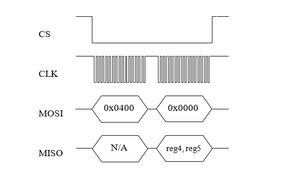
SPI master initiates a register read (for example register 0x04) by clocking in the address followed by 0x00, i.e. 0x0400, via MOSI. This combination is referred to as a read-command. It is followed by 16 zero-bits to complete the SPI data-transfer cycle. As the master transmits the read command over MOSI, the OpenIMU transmits information back over MISO.
In this transmission, the first data-word sent by the OpenIMU (as the read-command is sent) consists of 16-bits of non-applicable data. The subsequent 16-bit message contains information stored inside two consecutive registers (in this case registers 4 (MSB) and 5(LSB)).
Figure 1 illustrates register read over SPI interface:
4. OpenIMU SPI Block Mode Read Methodology
User can implement reading blocks of data with arbitrary length and information. Specific dedicated register address will indicate request specific block of data.
For example, register address 0x3e (62) indicates request for reading data block containing current data from unit sensors. Next table lists corresponding parameters:
Table 2. Block mode message format
Parameter Numer Size (bytes) Desctiption Status 2 Unit Status (see.p 10) X_Rate 2 Rate Sensor output (X) (64 LSB/deg/s) Y_Rate 2 Rate Sensor output (Y) (64 LSB/deg/s) Z_Rate 2 Rate Sensor output (Z) (64 LSB/deg/s) X_Accel 2 Accel Sensor output(X) (4000LSB/G) Y_Accel 2 Accel Sensor output(Y) (4000 LSB/G) Z_Accel 2 Accel Sensor output(Z) (4000 LSB/G) Temp 2 Unit Temperature
Read of data block begins when the master requests a read from specific register address (i.e. 0x3E). Figure 2 illustrates the read sequence:
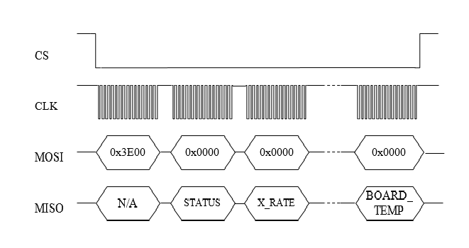
Note: Number of SPI clock pulses should be exactly equal to the length of predefined data packet (in this case – 144 (16 for address 128 for data)) otherwise interface may go out of sync.
For VG_AHRS/INS application examples next block message supported (register 0x3D):
Table 3. Extended VG block mode message format
Parameter Number Size (bytes) Description Status 2 Unit Status (see p.10) X_Rate 2 Rate Sensor output (X) (64 LSB/deg/s) Y_Rate 2 Rate Sensor output (Y) (64 LSB/deg/s) Z_Rate 2 Rate Sensor output (Z) (64 LSB/deg/s) X_Accel 2 Accel Sensor output(X) (4000LSB/G) Y_Accel 2 Accel Sensor output(Y) (4000 LSB/G) Z_Accel 2 Accel Sensor output(Z) (4000 LSB/G) Temp 2 Unit Temperature Roll 2 Unit Roll Angle (65536/(2*PI))LSB/RAD Pitch 2 Unit Pitch Angle (65536/(2*PI))LSB/RAD Yaw 2 Unit Yaw angle (65536/(2*PI)|LSB/RAD
For units with built-in magnetometer (OpenIMU330ZI) in some application examples next block message supported (register 0x3F):
Table 4. Extended MAG block mode message format
Parameter Number Size (bytes) Description Status 2 Unit Status see p.10 X_Rate 2 Rate Sensor output (X) (64 LSB/deg/s) Y_Rate 2 Rate Sensor output (Y) (64 LSB/deg/s) Z_Rate 2 Rate Sensor output (Z) (64 LSB/deg/s) X_Accel 2 Accel Sensor output(X) (4000LSB/G) Y_Accel 2 Accel Sensor output(Y) (4000 LSB/G) Z_Accel 2 Accel Sensor output(Z) (4000 LSB/G) Temp 2 Unit Temperature MAG_X 2 Mag sensor output (X) (16384 bits/Gauss) MAG_Y 2 Mag sensor output (Y) (16384 bits/Gauss) MAG_Z 2 Mag sensor output (Z) (16384 bits/Gauss)
5. OpenIMU SPI Register Write Methodology
The SPI master device can perform write into any register. The unit reaction on write operation is completely defined by the user. By default, corresponding data written without any reaction from unit. Written data can be read back. Unlike reads, writes are performed one byte at a time.
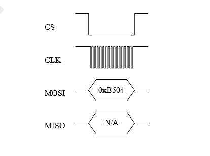
The following example highlights how write-commands are formed:
- Select the write address of the desired register, for example 0x35
- Change the most-significant bit of the register address to 1 (the write-bit), e.g. 0x35 becomes 0xB5
- Create the write command by appending the write-bit/address combination with the value to be written to the register (for example 0x04) - 0xB504
Figure 3 illustrates the register write over SPI:
6. OpenIMU Orientation programming
OpenIMU Orientation can be changed dynamically by writing corresponding values into the SPI registers 0x74 (MSB) and 0x75 (LSB). Data into register 0x74 should be written first. There are 24 possible orientation configurations (see below). Setting/Writing the field to anything else has no effect.
Table 5. OpenIMU Orientation field values
Registers 0x74/0x75 X Y Z 0x0000 +Ux +Uy +Uz 0x0009 -Ux -Uy +Uz 0x0023 -Uy +Ux +Uz 0x002A +Uy -Ux +Uz 0x0048 +Ux -Uy -Uz 0x0062 +Uy +Ux -Uz 0x006B -Uy -Ux -Uz 0x0085 -Uz +Uy +Ux 0x008C +Uz -Uy +Ux 0x0092 +Uy +Uz +Ux 0x009B -Uy -Uz +Ux 0x0041 -Ux +Uy -Uz 0x00C4 +Uz +Uy -Ux 0x00CD -Uz -Uy -Ux 0x00D3 -Uy +Uz -Ux 0x00DA +Uy -Uz -Ux 0x0111 -Ux +Uz +Uy 0x0118 +Ux -Uz +Uy 0x0124 +Uz +Ux +Uy 0x012D -Uz -Ux +Uy 0x0150 +Ux +Uz -Uy 0x0159 -Ux -Uz -Uy 0x0165 -Uz +Ux -Uy 0x016C +Uz -Ux -Uy
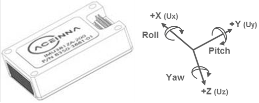
The default factory axis setting for the OpenIMU300ZI for SPI interface is (-Uy, -Ux, -Uz) which defines the connector pointing in the +Z direction and the +X direction going from the connector through the serial number label at the end of the unit. The user axis set (X, Y, Z) as defined by this field setting is depicted in figure below: Figure 4 illustrates unit orientation:
7. OpenIMU Digital Low Pass Filter selection
OpenIMU low pass filters can be changed dynamically for accelerometers and rate sensors writing corresponding values into the SPI registers 0x38 (for accelerometers) and 0x78 (for rate sensors). There are 11 possible low pass filter options (see below). Setting/Writing the field to anything else has no effect.
Table 6. OpenIMU Digital filter choices
Cutoff Frequency Filter Type 0x00 (0) N/A Unfiltered 0x03 (3) 40 Hz Bartlett 0x04 (4) 20 Hz Bartlett 0x05 (5) 10 Hz Bartlett 0x06 (6) 5 Hz Bartlett 0x30 (48) 50 Hz Butterworth 0x40 (64) 20 Hz Butterworth 0x50 (80) 10 Hz Butterworth 0x60 (96) 5 Hz Butterworth
8. OpenIMU DATA READY signal rate
OpenIMU DATA READY signal rate can be changed dynamically by writing corresponding values into the SPI register 0x37. There are 10 possible options (see below). Setting/Writing the field to anything else has no effect.
Table 7. OpenIMU SPI ODR Rate choices
0x00 (0) 0 0x01 (1) 200 Hz (default) 0x02 (2) 100 Hz 0x03 (3) 50 Hz 0x04 (4) 25 Hz 0x05 (5) 20 Hz 0x06 (6) 10 Hz 0x07 (7) 5 Hz 0x08 (8) 4 Hz 0x09 (9) 2 Hz
9. Saving unit configuration
Some configuration parameters can be saved in EEPROM and become active upon next unit restart (reset or power cycle). To save all parameters value 0 or 0xFF needs to be written to the register 0x76. It’s possible to save only specific parameter writing corresponding register address into register 0x76. Valid addresses are: 0x37, 0x38, 0x70, 0x71, 0x74, 0x75, 0x78.
10. Master Status Register
Master status register reflects current status of the unit. Next status indication bits are available:
Table 8. Master Status Register
Bit Status 0 Master Fail (1 - error) 1 HW Error (1 - error) 2 Reserved 3 SW Error (1 - error) 4 - 11 Reserved 12 Sensor Status (1 - error) 13 - 15 Reserved
11. HW Status Register
HW status register reflects current status of the unit. Next status indication bits are available:
Table 9. HW Status Status Register
Bit Status 0 - 1 Reserved 2 Sensor Error (1 - error) 3 Mag Error (1 - error) 4 Accel Error (1 - error) 5 Gyro Error (1 - error) 6 - 15 Reserved
12. SW Status Register
SW status register reflects current status of the unit. Next status indication bits are available:
Table 10. SW Status Status Register
Bit Status 0 Algorithm Error (1 - error) 1 Data Error (1 - error) 2 Cal CRC Error (1 - error) 3 - 15 Reserved
14. Accelerometer sensors scale factors and range
Next accelerometer scale factors and ranges are applicable:
Table 11. Accelerometer sensors scale factors and ranges
Unit Range & scale factor Value in register 0x70 Value in register 0x46 OpenIMU300ZI 8G , 4000 LSB/G 8 (r) 4 (r) OpenIMU330BI 8G , 4000 LSB/G 8 (r/w) 4 (r) OpenIMU330BI 16G , 2000 LSB/G 16 (r/w) 2 (r)
15. Rate sensors scale factors and range
Next rate sensors scale factors and ranges are applicable:
Table 11. Rate sensors scale factors and ranges
Unit Range & scale factor Value in register 0x71 Value in register 0x47 OpenIMU300ZI 500 dps, 64 LSB/dps 8 (r) 64 (r) OpenIMU330BI 500 dps, 64 LSB/dps 8 (r/w) 64 (r) OpenIMU330BI 1000 dps, 32 LSB/dps 16 (r/w) 32 (r) OpenIMU330BI 2000 dps, 16 LSB/dps 32 (r/w) 16 (r)
16. Suggested Operation
The following operational procedure and timing specifications should be adhered to while communicating with the OpenIMU300/OpenIMU330 via SPI interface to ensure proper system operation. These points are further highlighted later in this section.
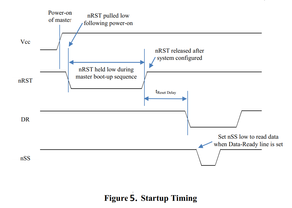
Startup Timing
The following timing applies at system startup (Figure 4):
- During system setup, the OpenIMU should be held in reset (nRST line held low) until the SPI master is configured and the system is ready to begin communications with the OpenIMU
- After releasing the reset line, the OpenIMU requires about 250-500 msec (tSystem Delay) before the system is ready for use
- Data best to be read from the OpenIMU right after falling edge of DATA REady signal. But at if readings are not synced to DATA READY signal - the latest available data sample sample will be provided.
Figure 5 illustrates OpenIMU startup timings:
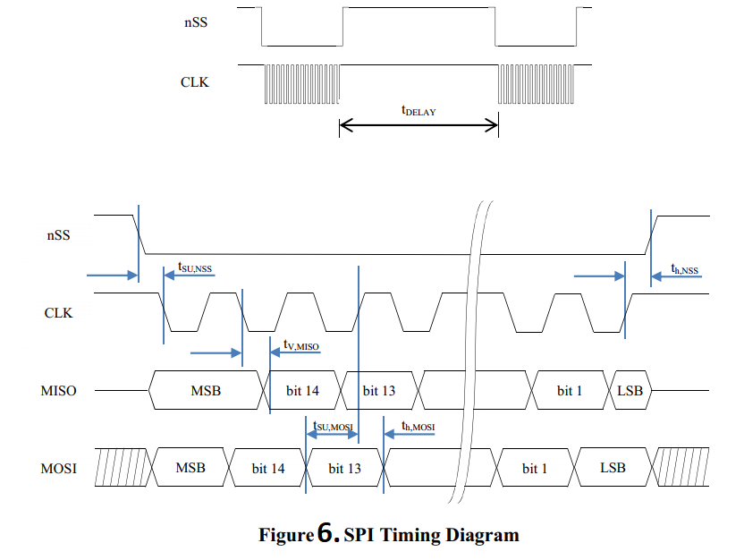
SPI Timings
The timing requirements for the SPI interface are listed in Table 12 and illustrated in Figure and Figure. In addition, the following operational constraints apply to the SPI communications:
- The unit operates with CPOL = 1 (polarity) and CPHA = 1 (phase)
- Data is transmitted 16-bits words, Most Significant Bit (MSB) first
Table 12. SPI Timing Requirements
Units SPI clock frequency 1 1.2 MHz 9 (min) 16 uSec 133 133 nSec 100 100 nSec 25 25 nSec 25 25 nSec 8 8 nSec
Figure 6 illustrates OpenIMU SPI bus timings: